 Follow Us on Google News
 Follow Us on Google Discover
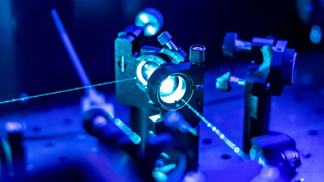
The field of integrated photonics has the potential to enable advancements in key technologies such as Quantum Computing, Light Detection and Ranging (LIDAR) for self-driving cars, and foster more energy-efficient data centres supporting the training of Artificial Intelligence (AI) models.
Furthermore, semiconductor electronics chips which have been the technological pillar of society, face limitations like heat generation. As demand surges for higher bandwidth and lower energy consumption, photonic chips provide an alternative solution.
‘Photonics’. ‘Integrated Photonics’. What does it all mean and why should you care?
Many individuals are likely familiar with electronic chips and the semiconductor industry with its applications in common everyday devices. The electronic semiconductor industry is one of the technological pillars of society, powering many prevalent devices, from laptops to mobile phones. These electronic chips of miniature size have an enormous impact on our day-to-day lives through the devices they help to operate.
The electronics industry has gone through several advancements since the 1940s to get it to where it is today. What if there was another similar technology, however a less mature one, that has the capability of powering a wave of frontier technologies, akin to what electronic semiconductors have done all these years?
Here enters Integrated Photonics.
Firstly, what is Photonics? When we speak of photonics, we are concerned with light.
Here, light does not only mean visible light that can be seen with a human eyebut also includes infrared and ultraviolet light and in other cases, other wavelengths on the electromagnetic spectrum.
While ‘electronics’ is the science of controlling electrons, the term ‘photonics’, analogously refers to the technology associated with controlling light. The term photonics was originally intended to depict a field that replaced functions typically achieved using electronics.
Photonics has to do with the technology, products, devices and processes that deal with the generation, transmission, transformation, detection and/or manipulation of light.
Before defining integrated photonics, it would be beneficial to understand bulk optics. Bulk optics has to do with large optical devices, which are devices for controlling and manipulating light (such as mirrors, filters, etc.). These are larger benchtop devices that you might find on the counter of a laboratory.
Compared to the larger size of devices in bulk optics, integrated photonics (also has been referred to as integrated optics) has to do with very small devices, allowing control of light on a nanoscale (one-billionth of a metre).
Integrated photonics can be defined as a branch of photonics or a technology focused on creating Photonics Integrated Circuits (PICs). PICs, also called photonic chips, consist of photonic components, which would have been much larger in size in bulk optics, but rather have been miniaturised and fabricated (meaning to manufacture) on the surface of a substrate like silicon. A substrate is a material or surface that serves as a foundation for components to be manufactured on.
Photonic components are like building blocks or pieces of a puzzle required to form functional photonic chips. Photonic components perform different functions, for instance, an example of a photonic component is a beam splitter (which splits light), and another is a grating coupler (which helps to couple, or put differently, direct light into a chip). Light entering the chip is supplied by a laser and is directed on chips within structures called waveguides, which also connect different photonics components.
Photonic components are designed to work for specific wavelengths or wavelength ranges of light. For instance, telecommunications and data communications, the largest field using PICs, make use of the 1550 nm and 1310 nm wavelengths of light.
Photonic components can be split into passive and active components. Passive components (such as multiplexers, couplers) do not require an external power source, while active components (like lasers and photodetectors) require an external power source.
Different materials can be used to create photonic chips. Popular material platforms are Silicon-on-Insulator, Silicon Nitride and Lithium Niobate.
Not only does integrated photonics significantly reduce the size of the components, it also reduces power consumption and boosts performance and reliability. Integrated photonics also provides the opportunity for large-scale production using semiconductor manufacturing techniques. These semiconductor manufacturing techniques are used in Silicon Photonics, a technology that makes use of Silicon-on-Insulator as the substrate.
Indeed, integrated photonics draws from the electronic semiconductor industry, as it can use the same scalable process to fabricate electronic chips, to make chips that work with light.
What about the difference between photonic chips and traditional electronic chips?Photonics chips are microchips that consist of photonics components arranged in a way to make a functional circuit. Photonics chips use light as the medium for transmitting data while electronic chips use electrons as the medium for transmitting data. Photonics offers benefits over electronics as light can transmit more data and generate less heat compare to electrons. Light particles, photons, do not collide with their transmitting medium the way electrons do in copper wire which results in heat.
The PICs market has been valued at about USD 14.51 billion in 2025 with growth forecasted (CAGR of 20.9 per cent from 2025 to 2032). Market growth is driven by the rising need for quicker data transmission rates, particularly in telecommunications and data centres.
A noteworthy trait about integrated photonics is its potential to enable other technologies. Take the example of quantum computers. Successful quantum computers can be used to speed up drug discovery due to the increased computational ability they enable. Integrated photonics can be used to make scalable quantum computers compared to the use of bulk optics.
PICs can support AI model operation as PICs can reduce power consumption, and lead to higher bandwidth (more data transmission per unit time) and lower latency (less delay in transmitting data) in data centres. Data centres are energy-intensive facilities that house IT equipment, store and process data. Data centres can consume up to 50 times more energy than an office space. In recent years, AI has been responsible for about 5-15 per cent of data centre power use and this figure could rise to 35-50 per cent by 2030. As photonics chips help to reduce energy consumption, they can help reduce the environmental impacts of AI in future scenarios that result in more emissions from AI.
LIDAR, which supports self-driving cars, uses a mechanical system to move a light source to scan the environment. Integrated photonics can be used to make LIDAR lighter, eliminate the moving part, and push down costs with high-volume photonics manufacturing. Integrated photonics can also lead to higher sensitivity with biosensors and can be used in other applications.
Before we end up with photonics products in the hands of consumers, several steps have to happen.
Idea. First, companies and individuals have an idea of the end product they would like to create that makes use of integrated photonics, such as quantum computers or biosensors.
Design. Next, comes the design stage. These companies that have the product idea can design their photonic components in-house or outsource the design to other companies. The circuits can be designed with packaging in mind at this stage to offer protection to the chips when finally manufactured. Once the components are designed using software and the components are laid out together into a functional circuit in the right way suited for the end application, then the designs are ready to be manufactured.
Manufacture. The circuit designs are then sent off to foundries/fabs who manufacture the chips. Hundreds of chips are typically manufactured together on a thin flat material called a wafer which can be diced after completion into different chips. The chips can be fabricated in Multi-Project Wafer (MPW) runs where chips are fabricated on predetermined time schedules on the same wafer shared with other users, which tends to make fabrication more cost-effective. Chips can also be fabricated with dedicated or custom runs, which are fabrication runs that can be for one user/organisation and can be more flexible in terms of timing.
Characterisation and packaging: Next, the chips are characterised (tested) to observe performance, and packaged to provide a scalable way to interface with your chips and offer protection.
The full cycle from idea to packaged chips can require iterations of some steps e.g. the fabricated chips do not have the intended performance thus the design is tweaked and fabricated again.
The overall cycle to get to functional chips can be a lengthy process, taking up to several months to possibly even years, and can be expensive, costing several tens or hundreds of thousands and could be up to millions of pounds. Improvements along the supply chain can help to speed up the time to fully functional chips.
Will integrated photonics replace electronic semiconductors? Despite its several benefits, photonics chips are unlikely to replace electronic chips completely. Integrated photonics has its own limitations. For instance, waveguides used to connect components cannot be smaller than the wavelength of light, thus limiting how small we can shrink these photonic chips without breakthrough solutions.
Instead of replacement, we can also look at further advancements in both fields and complementary solutions that maximise the benefits of both technologies to unlock new and improved applications.
Despite being a more nascent field than electronics, the future of integrated photonics looks luminous and further developments and investment in the field can prove beneficial for mankind.
I encourage the bright youth of Nigeria and other countries far and wide, to explore, learn more and actively contribute to the advancement of integrated photonics. This field is expected to grow, and has the ability and potential to significantly impact the future of our world.
Taiwo-Ashaju is an operations professional.